Nanotechnology Intruduction
Nanotechnology is the manipulation and engineering of materials at the atomic and molecular scale, typically within the range of 0.1 to 100 nanometers (nm). At this microscopic level, materials exhibit unique physical, chemical, and biological properties that differ significantly from their bulk counterparts. These exceptional properties are largely governed by the principles of quantum physics, which influence electron behavior, energy levels, and molecular interactions in ways that are not observed at larger scales.
An Interdisciplinary Field with Expansive Reach
Nanotechnology is inherently multidisciplinary, integrating knowledge and methodologies from various scientific and engineering domains. Fields such as applied physics, materials science, chemistry, biology, surface science, robotics, electrical engineering, and biomedical engineering contribute to the continuous evolution of nano technology. Over the past few decades, specialized subfields like nanoelectronics, nanomechanics, nanophotonics, and nanoionics have emerged, establishing a solid scientific foundation for nanoscale innovations.
The Origins and Evolution of Nanotechnology
The conceptual roots of nanotechnology can be traced back to a visionary lecture delivered in 1959 by renowned physicist Richard Feynman, titled “There’s Plenty of Room at the Bottom.” In this pioneering speech, Feynman speculated about the possibility of manipulating individual atoms and molecules to build new materials and devices, laying the groundwork for modern nanoscience.
The term “nanotechnology” was later coined by Japanese scientist Norio Taniguchi in 1974, further refining the field’s scope and definition. However, a major breakthrough occurred in 1981 with the invention of the scanning tunneling microscope (STM) by Gerd Binnig and Heinrich Rohrer. This revolutionary tool enabled scientists to visualize and manipulate individual atoms for the first time. The subsequent development of the atomic force microscope (AFM) provided even greater precision, accelerating research and practical applications.
The Unique Properties of Nanomaterials
Nanomaterials possess distinctive characteristics that set them apart from conventional materials. These properties arise due to:
- Size-dependent quantum effects: As particles shrink to the nanoscale, their electronic and optical properties change, leading to unique behaviors like quantum confinement and enhanced catalytic activity.
- Increased surface-area-to-volume ratio: Nanoparticles have a much larger surface area compared to their bulk equivalents, enhancing their reactivity, strength, and efficiency in applications such as catalysis and drug delivery.
- Enhanced mechanical, thermal, and electrical properties: Nanomaterials often exhibit superior strength, conductivity, and resistance to external stressors, making them highly valuable in engineering and medical applications.
Nanomaterials and Their Transformative Applications
Advancements in interface and colloid science have led to the creation of numerous nanomaterials, including:
- Carbon nanotubes (CNTs): Ultra-strong, lightweight structures with remarkable electrical and thermal conductivity, used in electronics, aerospace, and structural materials.
- Fullerenes (Buckyballs): Spherical carbon molecules with potential applications in superconductors, medical imaging, and drug delivery.
- Quantum dots: Semiconductor nanoparticles with unique optical properties, revolutionizing display technology, biological imaging, and solar energy applications.
- Nanoparticles: Engineered particles used in medicine, coatings, energy storage, and environmental remediation.
Impact of Nanotechnology Across Industries
Nanotechnology has revolutionized various industries, significantly enhancing efficiency, functionality, and innovation:
1. Medicine and Biotechnology (Nanomedicine)
- Targeted drug delivery systems improve treatment efficacy and reduce side effects.
- Biosensors detect diseases at an early stage with unprecedented precision.
- Tissue engineering benefits from nanoscale scaffolds that promote cellular regeneration.
2. Energy and Environment
- Nanopillars in solar cells reduce costs and improve efficiency over conventional silicon-based technology.
- Nanomaterials enhance energy storage devices, such as batteries and supercapacitors.
- Nanotechnology-based filtration systems purify water and improve environmental sustainability.
3. Electronics and Computing
- Nanoelectronics leverage miniaturized transistors for faster, more efficient computing.
- Flexible and lightweight nanomaterial-based displays are shaping the future of consumer electronics.
- Semiconductor nanoparticles contribute to advanced lighting technologies, including quantum-dot-based LEDs.
4. Materials Science and Manufacturing
- Nano-coatings provide enhanced durability and resistance in aerospace, automotive, and consumer goods.
- Self-healing materials utilize nanostructures to repair damage autonomously.
- Wear-resistant nanocomposites extend the lifespan of industrial components.
Nanotechnology Approaches: Bottom-Up vs. Top-Down
Nanotechnology employs two primary methodologies for designing and fabricating nanostructures:
- Bottom-Up Approach: This method involves constructing materials and devices from molecular components that self-assemble based on chemical interactions. It relies on principles of molecular recognition and is commonly used in nanochemistry and molecular nanotechnology.
- Top-Down Approach: This technique fabricates nano-objects from larger structures, often through lithography and etching processes. However, it lacks atomic-level precision compared to bottom-up methods.
The Future of Nanotechnology
The relentless progress in nanotechnology continues to push boundaries, unlocking new possibilities across multiple disciplines. Future advancements may include:
- Molecular nanorobotics: Miniature machines designed for medical applications, capable of repairing damaged tissues or targeting cancer cells at the molecular level.
- Self-assembling nanostructures: Materials that autonomously organize into functional devices, reducing production complexity.
- Quantum computing breakthroughs: Leveraging nanoscale quantum dots and superconducting materials for ultra-fast computation.
- Next-generation smart materials: Adaptive nanomaterials that respond dynamically to environmental changes, revolutionizing construction, textiles, and biomedical applications.
As nanotechnology continues to evolve, its potential to reshape industries and improve everyday life remains boundless. From healthcare innovations to sustainable energy solutions, the nanoscale revolution is poised to redefine the technological landscape of the future.
Applications of Nanotechnology:
Nanotechnology has revolutionized multiple industries by enabling precise control over materials and processes at the nanoscale. This technology leverages the unique properties of nanomaterials—such as enhanced strength, conductivity, reactivity, and biocompatibility—to develop groundbreaking solutions. Below is a detailed look at how nanotechnology is reshaping various sectors:
1. Health Sector: Revolutionizing Medicine and Biotechnology
Key Technologies:
- Targeted Drug Delivery Systems: Nanocarriers like liposomes and polymeric nanoparticles ensure precise drug delivery to diseased cells, minimizing side effects.
- Advanced Imaging Techniques: Gold nanoparticles enhance contrast in imaging techniques such as MRI and CT scans, leading to earlier and more accurate diagnoses.
- Tissue Engineering: Nanofibers and scaffold-based nanomaterials promote cell growth and regeneration, aiding in wound healing and organ replacement.
Scientific Principles:
- By utilizing nanoscale materials, these technologies interact with biological systems at the cellular and molecular levels, improving drug efficacy, precision, and treatment outcomes.
2. Food Industry: Enhancing Quality, Safety, and Sustainability
Key Technologies:
- Nano-Encapsulation: Protects flavors, nutrients, and bioactive compounds, ensuring prolonged freshness and controlled release.
- Nanosensors: Detect contaminants, spoilage, and bacterial presence in food, ensuring safety and quality.
- Nanotechnology-Enhanced Packaging: Nanomaterials with antimicrobial and oxygen-blocking properties extend shelf life and reduce food waste.
Scientific Principles:
- Nanomaterials improve food stability, enhance sensory attributes, and enable real-time monitoring of food quality through smart packaging.
3. Electronics: Driving the Future of Miniaturization and Performance
Key Technologies:
- Nanoscale Transistors: Allow for the creation of ultra-fast and compact processors in modern computing.
- Quantum Dot Displays: Nanoparticles improve brightness, color accuracy, and energy efficiency in display technologies.
- Enhanced Lithium-Ion Batteries: Nanomaterials improve battery capacity, longevity, and charging speed.
Scientific Principles:
- The integration of nanotechnology in electronics enhances conductivity, reduces power consumption, and enables the development of more compact and powerful devices.
4. Energy Efficiency: Pioneering Sustainable Solutions
Key Technologies:
- Nanocatalysts for Fuel Cells: Improve energy conversion efficiency by facilitating faster chemical reactions.
- Nanotechnology-Based Solar Cells: Quantum dots and nanowire technology enhance photovoltaic efficiency, reducing the cost of solar energy.
- Advanced Insulation Materials: Nanostructured coatings and aerogels optimize thermal resistance, reducing energy loss in buildings.
Scientific Principles:
- By improving energy conversion, storage, and insulation at the nanoscale, these innovations contribute to sustainable energy solutions and lower environmental impact.
5. Textiles: Smart Fabrics and Wearable Innovations
Key Technologies:
- Nano-Coatings for Water-Resistant Fabrics: Repel moisture, preventing damage and enhancing durability.
- Antimicrobial Textile Treatments: Silver nanoparticles prevent bacterial growth, keeping fabrics fresh and odor-free.
- Wearable Nanosensors: Integrated nanosensors monitor health metrics like heart rate, temperature, and hydration levels.
Scientific Principles:
- Nanotechnology provides textiles with enhanced properties such as self-cleaning, durability, and functionality in smart clothing.
6. Environment: Nanotechnology for Pollution Control and Sustainability
Key Technologies:
- Graphene-Based Water Purification Filters: Remove heavy metals, bacteria, and pollutants from drinking water.
- Nanoparticles for Environmental Cleanup: Magnetized nanoparticles absorb and extract oil spills or toxic substances from soil and water.
- Photocatalytic Materials: Break down pollutants and organic waste under sunlight, improving air and water quality.
Scientific Principles:
- By utilizing nanoscale interactions, these technologies enhance pollutant degradation and contribute to sustainable environmental solutions.
7. Transportation: Lightweight, High-Performance Materials
Key Technologies:
- Lightweight Nanocomposites: Used in vehicle frames, these materials reduce weight while maintaining strength, improving fuel efficiency.
- Nanomaterials in Electric Vehicle (EV) Batteries: Enhance energy density and lifespan, leading to longer battery life and faster charging times.
Scientific Principles:
- Nanomaterials optimize mechanical strength and conductivity while reducing energy consumption in transportation systems.
8. Space Exploration: Advanced Materials for the Future of Aerospace
Key Technologies:
- Radiation Protection Coatings: Shield astronauts and spacecraft from harmful cosmic radiation.
- Lightweight Nanocomposites: Reduce spacecraft weight while maintaining structural integrity, enhancing fuel efficiency and performance.
Scientific Principles:
- Nanotechnology contributes to the development of lightweight, durable, and radiation-resistant materials, essential for space exploration missions.
9. Nanorobots: A Breakthrough in Medical Microengineering
Key Technologies:
- Nanobots (~50–100 nm in size): Engineered for specific applications, such as targeted drug delivery, microsurgery, and cellular repair.
Scientific Principles:
- Nanorobots operate at the cellular level, enabling precise therapeutic interventions, such as detecting diseases, repairing tissues, or delivering drugs directly to cancerous cells.
10. Magnetic Hyperthermia-Mediated Cancer Therapy: A Novel Cancer Treatment
Process:
- Magnetic nanoparticles (typically iron oxide) are injected into tumor sites.
- An external alternating magnetic field is applied, causing the nanoparticles to generate heat.
- The heat destroys cancer cells while minimizing damage to surrounding healthy tissues.
Scientific Principles:
- The localized heating effect exploits magnetic field interactions at the nanoscale, providing a minimally invasive, highly targeted cancer treatment approach.
11. Agriculture: Precision Farming with Nanotechnology
Key Technologies:
- Nanocapsules for Targeted Delivery: Enhance the penetration of herbicides, fertilizers, and genes into plants, ensuring controlled release and minimal environmental pollution.
- Nanosensors for Soil and Plant Health: Detect soil nutrient levels, plant viruses, and environmental conditions in real time.
- Nano-Barcodes for Agricultural Monitoring: Track food quality and authenticity, ensuring supply chain transparency.
Scientific Principles:
- By integrating nanoscale technology, agriculture benefits from more efficient resource use, improved crop yields, and reduced environmental impact.
- Nanotechnology continues to drive innovation across diverse sectors, from healthcare and energy to agriculture and space exploration. By leveraging the unique properties of nanomaterials, industries can achieve enhanced efficiency, sustainability, and performance. As research advances, the future promises even more transformative breakthroughs, redefining how technology interacts with our world.
- Whether it’s the development of smarter medical treatments, cleaner energy solutions, or more efficient electronics, nanotechnology stands at the forefront of the next industrial revolution. Its applications are reshaping industries and improving lives on a global scale, proving that at the nanoscale, even the smallest innovations have the power to create monumental change.

Some examples of recent advances:
Nanotechnology has become a game-changer in modern medicine, offering revolutionary solutions for disease detection, treatment, and personalized healthcare. The ability to manipulate materials at the nanoscale has enabled scientists and medical professionals to develop highly targeted therapies, improve diagnostic precision, and enhance regenerative medicine. Below are some of the most promising applications of nanotechnology in healthcare, highlighting its transformative impact on patient care.
1. Cancer Detection and Treatment: Precision Oncology with Nanoparticles
Key Technologies:
- Gold Nanoparticles for Cancer Detection: Gold nanoparticles are used as molecular probes to detect specific nucleic acid sequences associated with cancer. These highly sensitive probes allow for early and accurate detection of cancerous cells, improving treatment outcomes.
- Nanoparticle-Based Therapies: Scientists are investigating the use of nanoparticles in clinical settings for direct cancer treatment, leveraging their ability to deliver therapeutic agents precisely to tumors.
Scientific Principles:
Nanoparticles interact with cancerous cells at the molecular level, allowing for high specificity in diagnosis and treatment. Their unique optical and chemical properties enable targeted imaging and therapy with minimal side effects.
2. Targeted Drug Delivery: Reducing Chemotherapy Toxicity
Key Technologies:
- Encapsulation of Chemotherapeutic Agents: Nanoparticles, including liposomes and polymeric carriers, can encapsulate cancer drugs and release them specifically at tumor sites.
- Minimizing Side Effects: By selectively targeting cancerous cells, nanomedicine reduces collateral damage to healthy tissues, significantly lowering the toxic effects of chemotherapy.
Scientific Principles:
Nanocarriers enhance the solubility, stability, and bioavailability of drugs while ensuring controlled and sustained drug release. This targeted approach reduces the systemic side effects associated with conventional treatments.
3. Advanced Imaging and Diagnostic Tools: Revolutionizing Medical Scanning
Key Technologies:
- Nanoparticle-Enhanced MRI and CT Scans: Contrast agents such as quantum dots and magnetic nanoparticles improve image resolution and provide real-time monitoring of disease progression.
- Early Disease Detection: Nanosensors and nanoprobes are being developed to detect biomarkers of diseases at an early stage, improving diagnostic accuracy.
Scientific Principles:
Nanotechnology enhances the sensitivity and specificity of imaging techniques, enabling earlier and more precise disease detection. These innovations pave the way for more personalized and effective treatment plans.
4. Cardiovascular Applications: Nanotechnology in Atherosclerosis Treatment
Key Technologies:
- Nanoparticles Mimicking High-Density Lipoproteins (HDL): Scientists have developed nanoparticles that mimic “good cholesterol” (HDL), which can help shrink arterial plaque.
- Nano-Enabled Stents: Drug-eluting stents with nanocoatings help prevent restenosis (re-narrowing of arteries) after surgical interventions.
Scientific Principles:
Nanomaterials interact with lipid deposits in arteries, enabling targeted plaque reduction while improving drug delivery to vascular tissues.
5. Genetic Engineering: Advanced DNA and Gene Sequencing
Key Technologies:
- Solid-State Nanopore Sequencing: Engineered nanopore materials allow for rapid, low-cost, and single-molecule gene sequencing.
- Gene Editing with Nanocarriers: Nanoparticles are being explored as delivery vehicles for CRISPR and other gene-editing technologies.
Scientific Principles:
By reducing sample preparation requirements and enhancing detection speed, nanopore technology simplifies genetic diagnostics and precision medicine applications.
6. Regenerative Medicine: Engineering the Future of Tissue Repair
Key Technologies:
- Nanostructured Bone and Neural Tissue Engineering: Nanomaterials are engineered to mimic the mineral structure of human bone, facilitating faster regeneration.
- Graphene Nanoribbons for Spinal Cord Repair: Conductive graphene nanomaterials promote neuron growth and nerve regeneration.
Scientific Principles:
Nanotechnology enables the creation of biomimetic materials that integrate seamlessly with human tissues, promoting self-repair and cell regeneration.
7. Vaccine Development: Innovations for Disease Prevention
Key Technologies:
- Nanoparticle-Based Vaccine Carriers: Nanoparticles improve vaccine stability, delivery, and immune response activation.
- Needle-Free Vaccines: Research is exploring nanotechnology-based vaccine delivery systems, such as nasal sprays and microneedle patches.
Scientific Principles:
Nanoparticles enhance antigen stability and immune response activation, reducing the need for traditional vaccine preservatives and improving efficacy.
8. Smart Pills: The Future of Personalized Medicine
Key Technologies:
- Electronic Capsules: Smart pills like the PillCam contain miniature video cameras for gastrointestinal imaging.
- Dose-Tracking Pills: Sensors within nano-enabled capsules monitor patient medication adherence in real time.
Scientific Principles:
Nano-electronic devices allow for real-time data collection, improving diagnostic capabilities and treatment monitoring.
9. Nanobots: Tiny Machines for Big Medical Breakthroughs
Key Technologies:
- Nanorobots as Miniature Surgeons: These microscopic devices can perform precision-based tasks such as repairing damaged tissues and delivering targeted drugs.
- Self-Replicating Nanobots: Future research aims to develop nanobots that can replicate within the body to correct genetic defects or eradicate diseases.
Scientific Principles:
Nanobots operate at the molecular level, offering highly precise therapeutic interventions with minimal invasiveness.
10. Nanofibers: Advanced Wound Healing and Surgical Applications
Key Technologies:
- Smart Bandages with Embedded Nanofibers: These bandages release clotting agents and antibiotics while monitoring wound conditions.
- Tissue Engineering and Artificial Organs: Nanofibers are used in scaffolds for organ regeneration and surgical implants.
Scientific Principles:
Nanofibers provide structural support for cell growth while delivering therapeutic agents directly to the wound site.
11. Nanotechnology in Pandemic Response: COVID-19 Detection and Treatment
Key Technologies:
- Nano-Based Diagnostic Tests: Metal and polymeric nanoparticles enhance the sensitivity of COVID-19 testing kits.
- Nano-Enabled Drug Delivery: Researchers are developing nanocarriers for antiviral drug delivery to target infected cells efficiently.
Scientific Principles:
Nanomaterials exhibit unique optical, electronic, and biochemical properties, making them highly effective in virus detection and treatment strategie
Nanotechnology is at the forefront of medical innovation, driving advancements in disease detection, treatment, and prevention. From targeted cancer therapies to next-generation vaccines, wearable health monitors, and self-repairing tissues, the potential of nanomedicine is vast.
As research and clinical applications continue to evolve, we move closer to a future where nanotechnology-powered healthcare solutions enhance human longevity, improve quality of life, and make medical treatments more efficient and accessible.
Nanosensors
Nanosensors are nanoscale devices that measure physical, chemical, or biological quantities and convert them into detectable signals. These advanced sensors play a crucial role in real-time monitoring, diagnostics, and environmental analysis, enabling precise measurements at the molecular and atomic levels.
As nanotechnology continues to evolve, nanosensors are becoming smaller, more sensitive, and more efficient, revolutionizing fields such as healthcare, environmental monitoring, industrial applications, and agriculture. Their ability to detect and analyze minute changes in their surroundings makes them indispensable for a variety of applications, from medical diagnostics to smart infrastructure monitoring.
Key Features of Nanosensors
1. High Sensitivity and Selectivity
- Nanosensors can detect substances at extremely low concentrations, making them ideal for early disease detection, pollution monitoring, and food safety testing.
- Their selective detection capabilities allow them to identify specific molecules, pathogens, or environmental pollutants with great precision.
2. Real-Time Monitoring and Fast Response
- Nanosensors provide instantaneous feedback, making them useful for continuous monitoring applications in healthcare, industry, and security.
- Their fast response times allow for quick decision-making in critical scenarios, such as disease outbreaks or hazardous material detection.
3. Miniaturization and Integration
- Due to their nano-scale size, these sensors can be integrated into wearable devices, implantable medical devices, and portable diagnostic tools.
- Nanosensors can be embedded in smartphones, lab-on-a-chip systems, and industrial automation systems for seamless data collection and analysis.
4. Advanced Fabrication Methods
- Nanosensors can be manufactured using a variety of techniques, including:
- Top-down lithography, which carves nanoscale features from bulk materials.
- Bottom-up self-assembly, where molecules or nanoparticles spontaneously organize into functional structures.
- Molecular self-assembly, which uses chemical interactions to form nanosensor components with atomic precision.
- Nanosensors can be manufactured using a variety of techniques, including:
Types of Nanosensors
1. Chemical Nanosensors
These sensors detect chemical substances at ultra-low concentrations.
- Used in pollution detection, water quality analysis, and gas sensing.
- Can detect toxic gases, heavy metals, and hazardous compounds in the environment.
- Used in food safety monitoring to detect contaminants and spoilage.
2. Biological Nanosensors (Biosensors)
These sensors detect biological molecules, including proteins, DNA, and pathogens.
- Used in medical diagnostics, such as early cancer detection, glucose monitoring for diabetes, and infectious disease screening.
- Play a key role in drug development and personalized medicine.
- Used in biological warfare detection and bioterrorism prevention.
3. Mechanical Nanosensors
These sensors measure physical parameters such as temperature, humidity, pressure, displacement, and vibrations.
- Used in smart buildings and industrial automation for structural health monitoring.
- Play a role in wearable fitness devices and implantable health monitors.
- Help in monitoring plant growth and metabolism in agriculture.
4. Optical Nanosensors
These sensors utilize light-based interactions to detect changes in the environment.
- Used in optical imaging for medical diagnostics.
- Applied in security and anti-counterfeiting measures.
- Used in astronomy and space exploration for advanced imaging techniques.
5. Magnetic Nanosensors
These sensors detect changes in magnetic fields.
- Used in magnetic resonance imaging (MRI) contrast agents for advanced medical imaging.
- Applied in data storage technologies and quantum computing.
Applications of Nanosensors
1. Medical Diagnostics and Neurophysiology
Nanosensors are transforming healthcare and medical diagnostics by providing early disease detection, personalized medicine, and real-time patient monitoring.
- Cancer Detection: Nanosensors can detect cancer biomarkers in blood samples, enabling early diagnosis and treatment.
- Glucose Monitoring: Nanosensors in wearable devices provide continuous blood sugar monitoring for diabetics.
- Brain Activity Monitoring: Nanosensors are used to analyze neural activity, advancing research in neurological disorders such as Alzheimer’s and Parkinson’s disease.
- Non-Invasive Health Monitoring: Wearable nanosensors provide real-time tracking of heart rate, oxygen levels, and hydration status.
2. Environmental and Pollution Monitoring
Nanosensors play a crucial role in detecting pollutants and ensuring environmental safety.
- Air Quality Monitoring: Nanosensors detect toxic gases, heavy metals, and particulate matter in the air, helping reduce pollution and health risks.
- Water Quality Testing: Used to detect contaminants such as lead, mercury, and bacteria in water supplies.
- Oil Spill Detection: Nanosensors help monitor oil spills and industrial waste leaks, assisting in environmental cleanup efforts.
3. Industrial and Structural Health Monitoring
Nanosensors are used in industrial automation, aerospace, and civil engineering for predictive maintenance and safety assessments.
- Bridge and Building Safety: Embedded nanosensors monitor stress, cracks, and corrosion in infrastructure to prevent failures.
- Smart Factories: Nanosensors enhance robotics and automation systems, improving efficiency and safety.
- Aerospace Applications: Used to monitor engine performance, temperature fluctuations, and material degradation in aircraft and space missions.
4. Smart Agriculture and Plant Biology
Nanosensors are being integrated into precision agriculture to optimize crop production and ensure food security.
- Soil Health Monitoring: Nanosensors detect nutrient levels, pH balance, and moisture content in soil.
- Crop Disease Detection: Helps in the early detection of plant diseases, preventing crop loss.
- Plant Metabolism Studies: Used in research to understand plant signaling pathways and improve genetic engineering of crops.
5. Security, Defense, and Anti-Terrorism
Nanosensors are valuable in homeland security and military applications for threat detection and surveillance.
- Explosive and Chemical Weapon Detection: Used to identify trace amounts of explosives and toxic gases in security-sensitive areas.
- Bioweapon Detection: Nanosensors can detect anthrax, viruses, and other biological threats in real time.
- Cybersecurity: Quantum nanosensors are being explored for unbreakable encryption in communication networks.

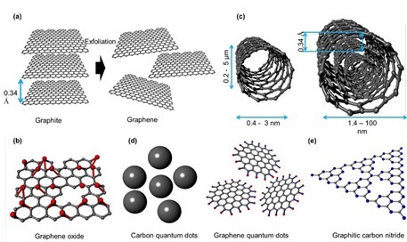
Graphene
- Graphene has been hailed as a “miracle material” in the global electronics industry due to its exceptional strength, high electrical conductivity, and incredible elasticity. Discovered in 2004, graphene has generated immense interest as a potential alternative to lithium-ion batteries and a revolutionary material for next-generation technology.
- Graphene is a single layer of carbon atoms arranged in a hexagonal lattice, making it an allotrope of carbon. This ultra-thin structure gives it remarkable mechanical, electrical, and thermal properties that surpass many existing materials. Despite being only one atom thick, graphene is 200 times stronger than steel, nearly transparent, and an excellent conductor of heat and electricity.
- Graphene serves as the fundamental building block of several other carbon-based materials, including graphite, charcoal, carbon nanotubes, and fullerenes. Its versatility and superior properties have positioned it as one of the most exciting materials in modern scientific research, with applications spanning from electronics to medicine and energy storage.
Exceptional Properties of Graphene
1. Unmatched Strength and Durability
- Graphene is the strongest material ever tested, capable of withstanding immense stress without breaking.
- Despite its strength, it remains incredibly flexible and lightweight, making it ideal for wearable electronics, aerospace engineering, and flexible displays.
2. Superior Electrical and Thermal Conductivity
- Graphene conducts electricity better than copper, allowing for faster and more efficient electronic circuits.
- Its high thermal conductivity makes it a promising material for cooling electronic devices and enhancing energy efficiency.
3. Transparency and Optoelectronic Advantages
- Graphene is nearly transparent, absorbing only about 2% of light, which makes it an ideal material for optical devices, touchscreens, and smart windows.
- Its ability to interact with light efficiently enables its use in high-performance LEDs, photodetectors, and lasers.
4. Potential to Revolutionize Energy Storage
- Graphene-based batteries and supercapacitors offer higher energy storage capacity, faster charging, and longer lifespan than traditional lithium-ion batteries.
- This has major implications for electric vehicles, smartphones, and renewable energy storage solutions.
Applications of Graphene Across Industries
Graphene’s unique properties make it an essential material in various cutting-edge technologies.
1. Electronics and Computing
- Graphene transistors can operate at much higher speeds than silicon-based transistors, paving the way for faster, more efficient computers and processors.
- Flexible and transparent electronics, including bendable screens and wearable technology, benefit from graphene’s strength and conductivity.
- Graphene-based ultrathin wires enhance circuit performance and reduce energy loss.
2. Energy Storage and Batteries
- Graphene supercapacitors store more energy, charge faster, and last longer than traditional electrolytic capacitors, making them ideal for renewable energy systems.
- Graphene-enhanced lithium-ion batteries offer higher efficiency, lower weight, and faster charging capabilities, improving performance in electric vehicles and mobile devices.
3. Solar Cells and Renewable Energy
- Graphene is used in next-generation solar panels, improving their efficiency and durability while reducing costs.
- Its transparency and conductivity make it ideal for flexible and lightweight solar cells, enabling solar energy integration into wearable tech and building materials.
4. Biomedical and Healthcare Innovations
- Due to its biocompatibility, graphene is being explored for use in biosensors, drug delivery systems, and tissue engineering.
- Graphene-based neural interfaces could enhance brain-computer communication, aiding in the development of advanced prosthetics and medical implants.
- Its antimicrobial properties make it useful for wound healing, antibacterial coatings, and next-generation medical devices.
5. Water Filtration and Purification
- Graphene oxide membranes can filter out even the smallest contaminants, including viruses, bacteria, and heavy metals, offering a cost-effective and sustainable water purification solution.
- Graphene’s hydrophobic properties allow for efficient desalination of seawater, addressing global water scarcity.
6. Sensors and Environmental Applications
- Graphene sensors are highly sensitive, enabling real-time detection of pollutants, toxins, and gases in the environment.
- These sensors can also be used in personalized healthcare, detecting diseases at an early stage through breath, sweat, or blood analysis.
7. Aerospace and Automotive Industries
- Graphene-reinforced composites can significantly reduce the weight of aircraft and automobiles, improving fuel efficiency and structural integrity.
- Heat-resistant graphene coatings protect spacecraft and satellites from extreme temperatures in space.
While graphene-based transistors are still in development, many experts believe that graphene will eventually replace silicon in key applications, leading to smaller, faster, and more energy-efficient electronics.
Challenges and Future of Graphene
- Despite its immense potential, graphene faces several challenges that must be addressed before widespread commercialization:
- High Production Costs
- Manufacturing high-quality, defect-free graphene at a large scale remains expensive and technically complex.
- Researchers are exploring cost-effective synthesis methods, such as chemical vapor deposition (CVD) and graphene oxide reduction.
- Integration into Existing Technologies
- While graphene is superior to silicon, integrating it into existing semiconductor manufacturing processes requires significant adaptation.
- Scientists are developing graphene-based hybrid materials that combine the benefits of graphene and silicon.
- Commercialization and Market Adoption
- Although graphene research has advanced rapidly, mass-market applications are still limited due to manufacturing constraints.
- Governments and private industries are investing heavily in graphene research, with ongoing projects aiming to make graphene-based products commercially viable.
The Graphene Revolution is Just Beginning
- Graphene’s unmatched properties make it one of the most promising materials of the 21st century. As researchers overcome production challenges, its applications in electronics, energy storage, medicine, and environmental solutions will continue to expand.
- From next-generation smartphones and flexible displays to high-capacity batteries and sustainable water filtration, graphene is set to transform industries and redefine technological possibilities. With ongoing advancements and large-scale investment, the dream of a graphene-powered future is rapidly becoming a reality.
.
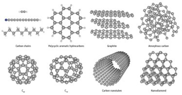
Carbon Nanotubes
Carbon nanotubes (CNTs) are an allotrope (Not isotope) of carbon.
Carbon nanotubes (CNTs) are cylindrical molecules made up of rolled-up sheets of single-layer carbon atoms (graphene). These nanostructures belong to the fullerene structural family, which also includes buckyballs (spherical carbon molecules). However, unlike buckyballs, carbon nanotubes have an elongated, tube-like shape with at least one end capped by a hemispherical structure.
With diameters as small as a few nanometers—nearly 50,000 times thinner than a human hair—carbon nanotubes can extend to several millimeters in length. This unique structural formation gives CNTs their extraordinary mechanical strength, high electrical conductivity, and efficient thermal properties.
Because of these remarkable attributes, CNTs have become one of the most promising materials in nanotechnology, with potential applications in electronics, optics, materials science, medicine, and energy storage.
Types of Carbon Nanotubes (CNTs)
Carbon nanotubes are primarily classified into two categories:
1. Single-Walled Nanotubes (SWNTs)
- Consist of a single layer of graphene rolled into a seamless cylinder.
- Diameter: Ranges between 0.4 to 2 nanometers.
- Unique electronic properties: Can behave as metallic or semiconducting materials, making them ideal for use in nanoelectronics and transistors.
- Highly flexible and mechanically stronger than multiwalled nanotubes.
2. Multiwalled Nanotubes (MWNTs)
- Composed of multiple concentric layers of graphene rolled into tubes, like a set of nested cylinders.
- Diameter: Typically 2 to 100 nanometers.
- More rigid and robust than SWNTs, but with slightly reduced flexibility.
- Excellent conductivity and used in applications such as high-strength composites and energy storage devices.
Exceptional Properties of Carbon Nanotubes
Carbon nanotubes exhibit unparalleled physical, electrical, and thermal properties, making them a revolutionary material for numerous technological advancements.
1. Extraordinary Mechanical Strength
- 50 times stronger than steel yet six times lighter, making CNTs an ideal reinforcement material for composites.
- Can be used in aerospace structures, bulletproof vests, and ultra-lightweight materials.
2. Unique Electrical Conductivity
- Depending on their structure, CNTs can behave as conductors or semiconductors.
- Can replace traditional silicon in nanoelectronics, transistors, and circuit components, enabling smaller, faster, and more efficient electronic devices.
3. Exceptional Thermal Conductivity
- Better heat conduction than copper, making CNTs valuable in cooling systems, heat sinks, and thermal coatings.
- Reduces overheating issues in electronic devices and batteries.
- Large Surface Area & High Aspect Ratio
- Due to their tube-like shape and nanometer-scale width, CNTs offer an exceptionally high surface area.
- This feature enhances their potential in chemical sensors, drug delivery systems, and energy storage applications.
Applications of Carbon Nanotubes Across Industries
1. Electronics & Semiconductors
- CNTs are seen as a potential replacement for silicon in transistors, allowing for the development of faster and more energy-efficient computers.
- Used in the production of flexible, transparent conductive films for touchscreens, displays, and smart windows.
- Quantum computing and nanowire interconnects benefit from CNTs’ superior electrical conductivity.
2. Energy Storage & Batteries
- CNT-based lithium-ion batteries offer faster charging, higher capacity, and a longer lifespan compared to traditional batteries.
- Used in supercapacitors that store and discharge energy more efficiently than conventional capacitors.
- Can improve the efficiency of solar cells and hydrogen fuel cells, advancing renewable energy technologies.
3. Aerospace & Automotive Industries
- Lightweight yet ultra-strong CNT composites help reduce fuel consumption in aircraft and automobiles.
- CNTs improve the strength and durability of carbon fiber-reinforced polymers used in satellites and space exploration vehicles.
- Thermal management applications help maintain optimal engine and battery temperatures.
4. Medicine & Biotechnology
- CNTs can act as drug delivery carriers, ensuring targeted delivery of medications to specific cells, minimizing side effects.
- Used in biosensors for detecting cancer markers, toxins, and pathogens.
- Enable neuronal regeneration and are being explored for brain-computer interfaces.
5. Water Filtration & Environmental Applications
- CNT membranes can filter out contaminants, heavy metals, and even salt molecules from water, making them ideal for desalination and purification systems.
- Can be used in air purification systems to remove pollutants and harmful gases.
6. Defense & Military
- CNT-based bulletproof materials provide higher durability and lower weight compared to traditional Kevlar.
- Used in stealth technology due to their ability to absorb electromagnetic waves.
7. Optics & Display Technology
- CNTs are used in next-generation flexible displays, enabling rollable and foldable screens.
- Their ability to emit electrons efficiently is being used in the development of field-emission displays (FEDs), a potential alternative to LCDs and OLEDs.
Challenges & Future of Carbon Nanotubes
Despite their remarkable potential, carbon nanotubes face certain challenges before widespread commercial adoption.
1. High Production Costs
- The cost of synthesis and purification of CNTs is still high, limiting large-scale production.
- Advances in chemical vapor deposition (CVD) and scalable manufacturing are addressing this issue.
2. Integration with Existing Technologies
- While CNTs offer better properties than traditional materials, integrating them into existing semiconductor and battery manufacturing processes remains a challenge.
3. Environmental & Health Concerns
- Some studies suggest that inhaled CNTs may have toxic effects, similar to asbestos.
- Researchers are working on biodegradable CNTs and safer handling protocols.
4. Controlled Synthesis
- Producing CNTs with specific properties (e.g., metallic vs. semiconducting behavior) is still difficult and requires precise structural control during synthesis.
Carbon nanotubes represent one of the most revolutionary advancements in nanotechnology. Their unmatched strength, electrical properties, and thermal conductivity make them a game-changer across multiple industries, from electronics and energy storage to aerospace and medicine.
With ongoing technological advancements, cost-effective production techniques, and further research into biocompatibility and safety, CNTs are poised to reshape the future of materials science.